Application
Comprehensive 3D Characterization of Complex Dislocation Arrangements in Silicon Wafers
X-ray diffraction laminography (XDL) has been applied to silicon (Si) wafer samples with considerable lateral extension like typical industrial wafers. By combining XDL with X-ray white-beam topography (XWBT) and (circularly polarized) visible light differential interference contrast (CDIC) microscopy a comprehensive characterization of complex 3D dislocation structures was obtained, see Fig. 1 [Hänschke 2017, 2018, Horton 2017, Redmond 2018]. The 3D paths of the individual dislocations could be resolved with a resolution of about 3 micrometer, the associated Burgers vector distribution could be determined, and the bulk features could be linked to corresponding surface features like surface steps or mechanical damage.

alternating with heating cycles. b) Visualization
of selected individual 3D dislocation paths and
the associated Burgers vectors
indicated by color.
Quasi 4D Imaging of Dislocation Dynamics in Silicon
The nucleation, propagation, and interaction of dislocations within complex arrangements in silicon were observed by performing a gradual annealing alternating with 3D XDL scans.
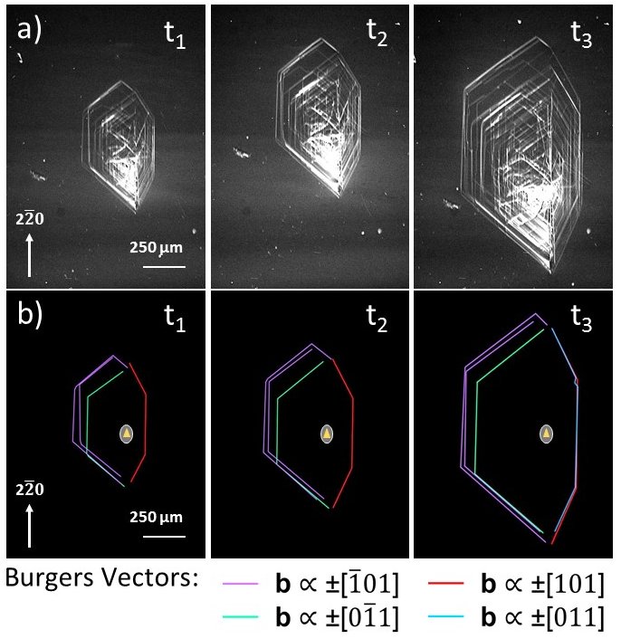
Industrial Si wafer samples with prior mechanical nano-indentations were heated above the brittle-to-ductile transition temperature (for Si 600°- 700°C) with suitable temperature gradients by utilizing a double ellipsoidal mirror oven. During these thermal treatments, dislocations emerge from the mechanical damage and expand into the crystal volume. Fig. 2 shows XDL projections for similar view angles illustrating the evolution after two annealing steps (t1<t2<t3).
Based on these XDL data, the 3D volume was reconstructed and quantitative information has been extracted about the development of thermally driven dislocations. For example, Fig. 3 shows the determined evolution of one selected individual dislocation half loop.
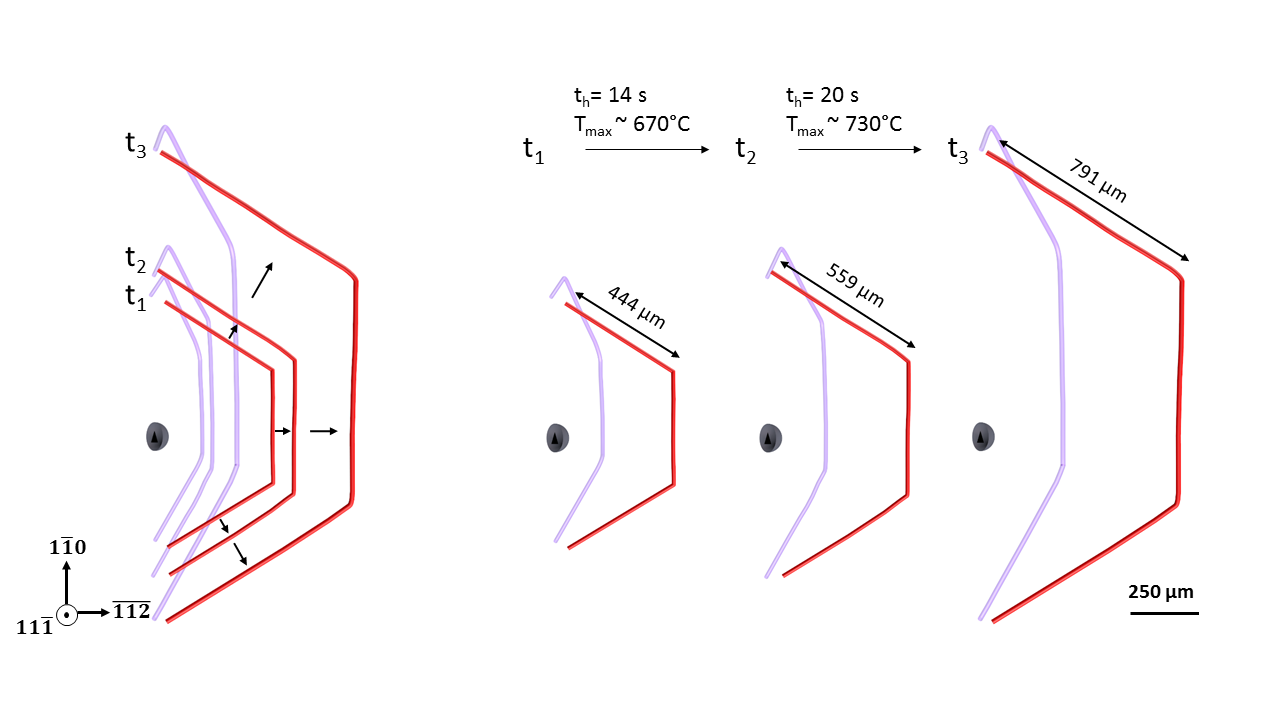
Fig. 3: View on the evolution of two segmented dislocations on different slip planes and the length of the segments analyzed in 3D after gradual annealing.
Thermographic monitoring of the samples in real time using and infrared camera provides new possibilities. Within the STROBOS-CODE project, tools for such data analysis of quasi in-situ 3D data have been refined and the relation between the observed 3D dislocation dynamics and the driving shear sress acting in the various {111}<110> slip systems has been investigated, see Fig. 4.

Fig. 4: Left: 3D segmentation of the XDL measurement after the final annealing cycle of a complex dislocation structures around different sources (5 indents) in a silicon wafer, including Burgers vector distribution (color-coded). Right: Resolved shear stress simulations for various {111}<110> slip systems in the crystal area around the investigated dislocation structures. The low values of the calculated resolved shear stress (top row) are directly related the lack of corresponding dislocations.
Application of XDL for the Investigation of Dislocation Cell Walls and Small-Angle Grain Boundaries in GaAs and CdTe
The project partners successfully applied XDL to the higher-Z semiconductor materials GaAs and CdTe to characterize different types of crystalline defects.
The strain fields around two indents on a GaAs wafer are clearly visible in the weak beam XDL projection displayed in the left image of Fig. 5. These indents are imbedded in a network of dislocations, forming cellular structures of strain fields. In the center of Fig. 5 such cellular dislocation networks are shown in a 3D rendered XDL reconstruction. During the algebraic reconstruction process the so called weak beam contrast has been inverted.
Unlike the two other images the contrast mechanism in the right image of Fig. 5 is the so-called integrated intensity contrast. With this kind of diffraction contrast it was possible to reveal small angle grain boundaries within the bulk of a CdTe wafer.
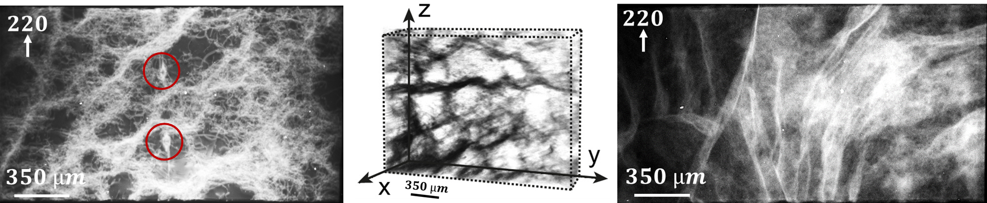
Center: Image of a 3D reconstruction volume rendering of a cellular dislocation network in a GaAs wafer (defects are dark).
Right: Integrated intensity image showing small angle grain boundaries within a CdTe wafer.
